MP Board Class 12th Physics Important Questions Chapter 14 Semiconductor Electronics: Materials, Devices and Simple Circuits
Semiconductor Electronics: Materials, Devices and Simple Circuits Important Questions
Semiconductor Electronics: Materials, Devices and Simple Circuits Objective Type Questions
Question 1.
Choose the correct answer of the following:
Question 1.
The forbidden energy gap in Germanium crystal is :
(a) 1.2 x 10⁻¹⁹J
(b) 1.76 x 10⁻¹⁹J
(c) 1.6 x 10⁻¹⁹J
(d) Zero
Answer:
(a) 1.2 x 10⁻¹⁹J
Question 2.
The valency of impurity dopped in a pure germanium crystal to make it P – type semiconductor is:
(a) 3
(b) 4
(c) 5
(d) 6
Answer:
(a) 3
Question 3.
The deplection layer of P – N junction has :
(a) Electrons
(b) Protons
(c) Mobile ions
(d) Immobile ions
Answer:
(d) Immobile ions
![]()
Question 4.
The width of deplection layer in P-N junction diode is
(a) 10-3 m
(b) 10-4 m
(c) 10-5 m
(d) 10-6 m
Answer:
(d) 10-6 m
Question 5.
Zener diode is used as :
(a) Amplifier
(b) Rectifier
(c) Oscillator
(d) Voltage regulation
Answer:
(d) Voltage regulation
Question 6.
Light emitting diode is formed by :
(a) Silicon
(b) Germanium
(c) Carbon
(d) Ga – As
Answer:
(d) Ga – As
Question 7.
Which of the following is a photo voltaic device :
(a) Photo cell
(b) LED
(c) Zener diode
(d) Solar cell
Answer:
(d) Solar cell
Question 8.
When N – P – N transistor is used as amplifier then :
(a) Electrons goes from base to collector
(b) Holes goes from emitter to base
(c) Holes goes from collector to base
(d) Holes goes from base to emitter.
Answer:
(a) Electrons goes from base to collector
Question 9.
The relation between current gain in CB mode (α) and current gain (β) in CE mode is:
(a) β = α + 1
(b) β = \(\frac {α}{1 – α}\)
(c) β = \(\frac {α}{1 + α}\)
(d) β = 1 – α.
Answer:
(b) β = \(\frac {α}{1 – α}\)
Question 10.
In CE amplifier the phase difference between input and output signals is :
(a) 0°
(b) 90°
(c) 180°
(d) 270°.
Answer:
(c) 180°
![]()
Question 11.
Oscillator is an amplifier with :
(a) Positive feed back
(b) Negative feed back
(c) No feed back
(d) High current gain.
Answer:
(a) Positive feed back
Question 12.
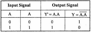
The boolean expression for NAND gate is :
(a) A + B = Y
(b) A – B = Y
(c) A = Y
(d) AB = Y.
Answer:
(d) AB = Y.
Question 2.
Match the Column :
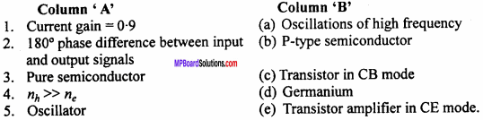
Answer:
- (c)
- (e)
- (d)
- (b)
- (a)
Question 3.
Fill in the blanks :
- Zenar diode is used as ……………..
- The ratio of change in output voltage to change in the input Voltage is called ……………..
- Power gain = (Current gain)2 x ……………..
- With increase in temperature of a semiconductor its conductivity ……………..
- In an intrinsic semiconducter the forbidden energy gap is of order of ……………..
- Main function of a tank circuit is to produced ……………..
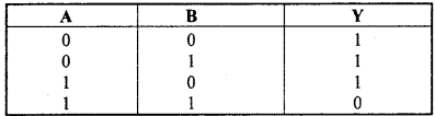
- In a NAND gate there is a …………….. gate along with AND gate.
- NOT gate is also called as ……………..
- The boolean expression of AND gate is ……………..
- If Y = \(\overline {A+B}\) then gate is ……………..
- Photo diode is used as ……………..
- Light emitting diode is used in …………..
Answer:
- Voltage regulation
- Voltage gain
- Resistance gain
- Increases
- 1 eV
- Oscillations
- NOT
- Inverter
- Y = A.B
- NOR
- To defect light
- Light emission.
Question 4.
Write the answer in one word/sentence :
- How does the energy gap in the intrinsic semiconductor varies on introducing a penta valent impurity in it?
- Whose drift velocity is greater holes or electrons.
- On increasing the reverse bias in P – N junction diode how does the width of depletion layer vary?
- In which bias the resistance of P – N junction diode is very high?
- What is use of zener diode?
- A transistor is used as an amplifier in common emitter mode rather than in common base mode why?
Answer:
- The energy gap decreases
- The drift velocity of electrons is greater than that of holes
- The width of depletion layer increases
- Reverse bias.
- It is used as voltage regulator
- Because in common emitter amplifier the voltage gain and power gain is more.
Semiconductor Electronics: Materials, Devices and Simple Circuits Very Short Answer Type Questions
Question 1.
What are semiconductors? Write down names of any two semiconductors.
Answer:
The substances which have electrical conductivity between conductors and insulators are called semiconductors.
Examples:
Germanium, silicon.
Question 2.
How does the conductivity of semiconductors affected on heating the semi – conductors?
Answer:
When a semiconductors is heated then the covalent bond get broken and the valence electrons becomes free. With increase in temperature the number of free electrons increases. Hence the conductivity of semiconductor increases.
Question 3.
Choose the conductor, insulator and semiconductors in the following : Germanium, Tungsten, Air, Silver, Silicon, Carbon.
Answer:
- Conductor : Tungsten, Silver.
- Insulator : Air
- Semiconductor : Germanium, Carbon, Silicon.
![]()
Question 4.
Write difference between the charge occurs in the resistivity of metals and intrinsic semiconductor with temperature.
Answer:
With increase in the temperature the resistivity of metals increases while that of intrinsic semiconductor decreases.
Question 5.
Draw the symbol of P – N junction diode.
Answer:
Question 6.
How can a pure semiconductor be converted into a P – type semiconductor?
Answer:
When a trivalent impurity such as indium, boron etc are introduced into pure semiconductor then P – type semiconductor is formed.
Question 7.
How can a pure semiconductor be converted into a N – type semiconductor?
Answer:
When a pentavalent impurity such as antimeny, arsenic phosphorus etc. are introduced into pure semiconductor then N – type semiconductor is formed.
Question 8.
What is the ratio of number of holes to number of electrons in an intrinsic semiconductor?
Answer:
1 : 1.
Question 9.
Write the name of majority charge carriers in P – type and N – type semiconductors.
Answer:
In P – type semiconductor majority charge carriers are holes and in , N – type semiconductor majority charge carriers are electrons.
Question 10.
What is LED?
Answer:
It is Abbreviation of ‘Light Emitting Diode’. It is a P – N junction which, when used in reverse bias, emits the light.
![]()
Question 11.
In a transistor emitter is always forward biased and collector is reverse biased, why?
Answer:
The charge carriers (electrons or holes) are moved only when the emitter is forward biased while collector will occupy them only when it is reverse biased. So that there is a unidirectional flow of current.
Question 12.
What are universal gate?
Answer:
NOR gate and NAND gate are called as universal gate, because by the combination of these gates, other logic gates can be obtained.
Question 13.
What is dopping? Why it is necessary?
Answer:
The process of introducing the impurities in a pure semiconductor is called dopping. To form N – type and P – type semiconductors dopping is necessary.
Semiconductor Electronics: Materials, Devices and Simple Circuits Short Answer Type Questions
Question 1.
What do you understand by intrinsic and extrinsic semiconductors?
Answer:
Intrinsic semiconductors:
Pure semiconductors are called intrinsic semiconductors example germanium and silicon. The number of electrons and holes are equal in it.
Extrinsic semiconductors:
The semiconductors containing impurities of pentavalent or trivalent substances are called extrinsic semiconductors. The electron density is not equal to hole density.
Question 2.
Semiconductors are used to form the transistor. Why?
Answer:
Transistor are made by N – type and P – type semiconductors where the charge carriers are electrons and holes. Thus, the function of transistor is based on the control over the motion of electrons and holes. This control is not possible in conductors and insulators. Therefore only semiconductors are used to make transistors.
Question 3.
Explain the meaning of word “Transistor”.
Answer:
Transistor is a short form of transformation of resistance. The low resistance of forward biased junction is transformed to high resistance of reverse biased junction. Therefore it is called as transistor.
![]()
Question 4.
Why the base is designed thin in comparison to emitter and collector in a transistor?
Answer:
A thin and lightly doped base region will contain a smaller number of majority charge carriers. This will reduce the recombination rate of electrons and holes when major-ity charge carriers move from emitter to collector.
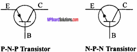
Question 5.
Draw symbols of P – N – P and N – P – N transistors.
Answer:
P – N – P Transistor N – P – N Transistor
Question 6.
What is difference between transformer and transistor?
Answer:
The transformer changes alternating voltage but the power remains same. Amplifier increases power of alternating voltage.
Question 7.
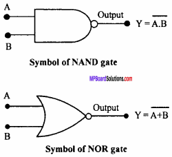
Draw symbol of NAND and NOR gate.
Answer:
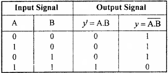
Question 8.
What is Universal gate? Why they are called so?
Answer:
NOR and NAND gates are called as universal gates because by the combination of these gates other gates can be formed.
Question 9.
How will you obtain NOT gate from NAND gate? Draw logic symbol and write truth table.
Answer:
When the two input signal of NAND gate are joined together then the output signal obtained is equivalent to that of NOT gate.
Symbol :
![]()
Truth table:
Question 10.
How will you obtain AND gate from NOR gate?
Answer:
To obtain AND gate from NOR gate:
If the output of two NOT gate obtained by NOR gates are used as two inputs of a NOR gate then the resultants output be same as the output of AND gate.
Symbol:
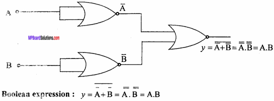
Truth table:
Question 11.
How will you obtain OR gate from NAND gate?
Answer:
If the two outputs of NOT gates obtained by NAND gates are used as inputs of a NAND gate then the final output be same as the output of OR gate.
Symbol:
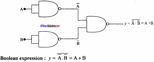
Truth table:
Question 12.
What is dopping? Why it is necessary?
Answer:
The process of introducing the impurities in a pure semiconductor is called dopping. To form N – type and P – type semiconductors dopping is necessary.
Question 13.
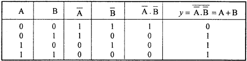
Identify the following symbol, write its boolean expression and write the truth table:
Answer:
It is a NAND gate.
Boolean expression : y = \(\overline { A.B } \quad\)
Truth table:
Question 14.
Explain the following terms with reference to a P – N junction :
- Uncovered charge
- Depletion layer
- Potential barrier.
Answer:
1. Uncovered charge : The positive immobile ions present on the N – region and negative immobile ions present in P – region near the junction are called uncovered charge.
2. Depletion layer : The layer on either side of P – N junction which does not contain any charge carrier (neither positive charge carrier nor negative charge carrier) is called depletion layer.
3. Potential barrier : The potential difference developed across the depletion layer is called the potential barrier.
Question 15.
What is P – N diode? Explain the formation of depletion layer in it.
Answer:
When P – type semiconductor is joined with N – type semiconductor by some special techniques as etching or sandwitching, then the junction formed is called P – N diode. It works similar to that of diode valve. Hence, it is called P – N junction diode. When P – N junction diode is made, then free electrons present in N – type get diffused across the boundary into P – type and few number of holes diffuse into N – type from P – type. Thus, a thin film (less than 10-3 cm) at the junction becomes free from holes and electrons. This thin film is called depletion layer.
![]()
Question 16.
What is zener diode? Explain it.
Answer:
Zener diode is P – N junction diode which is fabricated for a definite breakdown voltage. The value of breakdown voltage depend upon the doping density of P – and ,V – type semiconductor. The breakdown voltage depends upon the concentration of doping, in a highly dopped P – N junction, the depletion layer is very thin so that the value of zener voltage becomes very small.
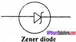
For a definite breakdowm voltage zener diode ner diode is constructed by a special doping in such a way that it doesn’t get damaged even it working at breakdown voltage at reverse bias.
Symbol:
The symbol of zener diode is shown in adjacent fig.
Principle:
In the reverse biased zener diode, on applying breakdown voltage it allows easy flow of current. But inspite of flow of current the P – N junction do not get de – stroyed. When the applied voltage becomes less than breakdown voltage it again becomes a normal P – N junction diode.
Use:
It is used as voltage regulator.
![]()
Question 17.
What is a Solar cell?
Or
How a junction diode can be used as a solar cell?
Answer:
Solar cell:
It is a P – N junction diode which converts the solar energy into electrical energy. It works on the principle of photoelectric effect.
When the solar light fall on the P – N junction then an e.m.f. is produced across its ends. This e.m.f. is called as photoelectric e.m.f. Hence a P – N junction acts as source of e.m.f. This is called solar cell.
Working:
When light photons reach the junction they excite electrons from the valence band to conduction band leaving behind equal number of holes in the valence band. The electron hole pairs generated in the deplection region move in opposite directions due to the barrier field. Photo generated electrons move towards N – region and holes towards P – region.
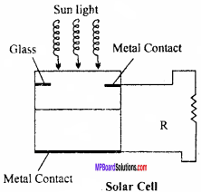
The collection of these charge carriers make P – region positive electrode and N – region a negative electrode. Hence photovoltage is set up across the junction. When a load resistance R is connected in the external circuit, a photo current I flows through it.
Question 18.
Explain the working of N – P – N transistor with labelled diagram.
Answer:
The adjacent fig. shows the N – P – N transistor in CE mode.
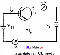
The emitter is at negative potential w.r.t. the base and collector. The electron of emitter region are repelled by the negative terminal of the battery VBE and move towards the base region, as the base region is very thin most of the electrons cross this region and enter to the collector region. Only 2% to 5% of electrons combine with the holes present in base region, therefore Ib the base current flows. The electrons entering into collector region are attracted very fast by the positive terminal of battery VCE and collector current Ic flows through the external circuit.
If the emitter current is Ie then by Kirchhoff’s law
Ie = Ib + Ic
Semiconductor Electronics: Materials, Devices and Simple Circuits Long Answer Type Questions
Question 1.
Explain P – type semiconductors in terms of energy band.
Answer:
When a trivalent impurity (Such as Boron, Aluminium etc.) is introduced (dopped) in a pure Ge crystal then a P – type semiconductor is formed.
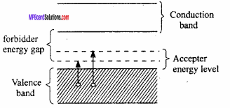
In a P – type semiconductor each acceptor impurity atom process a hole. This hole is fulfilled by an electron of nearest Ge – Ge band. To remove the electron from covalent band and to bring it to the hole very small amount of energy (about 0.01 – 0.05 eV) is required. Hence the acceptor energy level is slightly above the top of valence band. At room temperature the electrons of valence band get excited and reach to the acceptor level. Therefore same number of holes are created in valence band. Thus in P- type semiconductor the number of holes in valence band is much greater than the number of electron in conduction band.
Question 2.
What do you understand by N – type and P – type semiconductors? Give differences between them.
Or
Differentiate between the P – type and N – type semiconductors.
Answer:
N – type : When pure germanium is introduced by small amount of a pentavalent atoms as antimony, arsenic, etc. then N – type semiconductors are formed.
P – type : When pure germanium is introduced by small amount of a trivalent atoms as indium, boron, etc. then P – type semiconductors are formed.
Difference between N – type and P – type semiconductors :
N – type:
- N – type of semiconductors are formed by the impurities of pentavalent elements.
- Electrons are the charge carriers.
- Number of electrons in conduction band is greater than the number of holes in valence band.
- Fermi level is towards conduction band.
P – type:
- P – type of semiconductors are formed by the impurities of trivalent elements.
- Holes are the charge carriers.
- Number of holes in valence band is greater than the number of electrons in conduction band.
- Fermi level is towards valence band.
![]()
Question 3.
Explain working of P – N – P transistor in CE mode.
Answer:
Working of P – N – P transistor :
The figure shows the common emitter circuit. The emitter is at positive potential w.r.t. the potential of base and collector. The holes coming from the emitter are only 2% to 5% which combine in the base region thus low current is flown in emitter circuit and other holes are attracted by the negative terminal of the battery Vce.
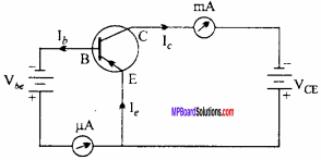
As soon as the hole reaches to the end, the electron from the negative terminal of the battery Vce neutralizes it and at the same time, a covalent band breaks at emitter region. Thus, an electron enters the positive terminal of the battery Vbe and the same process is repeated. Thus, the current flows through P – N – P transistor by holes and outside it in external circuit by electrons. If the emitter current be Ie. Then, Ie = Ib + Ic.
Question 4.
Explain with a circuit diagram, how common emitter P – N – P transistor is used as amplifier?
Or
Explain the working of P – N – P transistor as amplifier in CE mode with a circuit diagram.
Answer:
In concerning circuit use of transistor as an amplifier is shown :
Where, S → Input signal, R → Load resistance, Vc → Collector voltage. In this circuit, emitter is kept at positive potential relative to the base and collector. Input signal is applied between base and emitter. Load resistance R is added to the collector circuit.
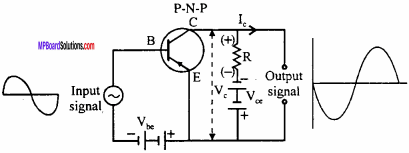
As a result collector becomes more negative and output signal becomes negative. In next half cycle of input signal, potential of base becomes more negative relative to emitter and Ic increases, therefore value of collector voltage Vc decreases or it becomes negative which gives positive output signal.
In this way, opposite signals are obtained in different half cycles of input signal. So, it is clear that there is phase difference of 180° between the input and output signals.
Question 5.
Explain the working of N-P-N transistor as amplifier in CE mode under following points :
- Circuit diagram
- Working
- Voltage gain.
Answer:
1. Circuit diagram :
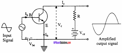
2. Working:
The emitter terminal is common to both the input and output circuit. While the input circuit is forward – biased, the output circuit is reverse – biased.
When no a.c. signal (input) is supplied to the input, the collector current Ic flows through load resistance (R) will produce a voltage drop Ic R across R. Hence, the net output voltage is
Vc =Vce – Ic R … (1)
Suppose the signal to be amplified is now fed the input circuit. During the positive half cycle of input, the forward bias of base – emitter increases. So, emitter and collector current increases. Hence, from equation (1), Vc decreases. But Vc is joined to high potential, so high potential value decreases. So, amplified signal becomes negative. This explains the amplification of positive half cycle.
During the negative half cycle of input, forward bias decreases both emitter and collector current decreases, hence Vc increases by equation (1). So, the output becomes more positive. Clearly, the output signal is 180° out of phase from the input signal.
3. Voltage gain:
The ratio of change in output voltage to the change in input voltage is called voltage gain. It is denoted by Av.
Question 6.
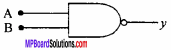
What is NAND gate? Write its symbol, truth table and boolean expression.
Answer:
When a NOT gate is connected at the output of AND gate then the logic gate formed is known as NAND gate.
Symbol:
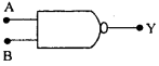
Truth Table:
Boolean expression : \(\overline { A.B } \quad\) = Y.
Question 7.
Explain NOT gate under the following heads :
- Symbol
- Relation between input and output
- Equivalent circuit.
Answer:
1. Symbol:
![]()
2. Relation between input and output : Y = \(\overline { A}\), where Y is output and A is input.
3. Equivalent circuit:

Question 8.
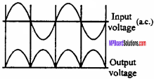
What is rectification? Explain half – wave rectification by diode on the basis of following points:
- Labelled diagram of circuit
- Working
Or
Describe the use of P – N junction diode as half wave rectifier under the following heads:
- Labelled circuit diagram
- Working
- Graph for time variation of input and output potential.
Answer:
Rectification:
The phenomenon of conversion of a.c. to d.c. is known as rectification.
1. Labelled diagram:
a.c. → Input a.c. voltage, T → Step – up transformer, PN → Junction diode, R → Load.
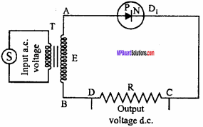
2. Working:
When an a.c. voltage is applied to the primary coil of transformer, then an a.c. voltage is induced in the secondary coil of transformer. Let in half cycle, A is at positive potential w.r.t. that of B. Then P – N junction diode is in forward – biased. Thus, the current flows through it and conventional cunrent flows through R, from C to D.
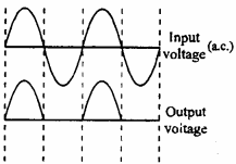
In the next half cycle, A is at negative potential w.r.t. B. The junction diode is in reverse – biased and no current flows through R. The same phenomenon is repeated in the next cycle. Therefore, only half cycle of the input a.c. wave is converted into d.c. This process is called half – wave rectification.
Question 9.
What is rectification? Drawing the electrical circuit show a P – N diode can be used as full wave rectifier.
or
Describe the use of P – N junction diode as a full wave rectifier under the following heads:
- Labelled circuit diagram
- Working
- Wave form of output signals.
Or
What is a rectifier? Draw circuit diagram to explain the use of P – N junction diode as full wave rectifier.
Answer:
The process of converting the alternating current into direct current is called rectification and the circuit used for the purpose of rectification is called rectifier circuit.
1. Labelled diagram :
T → Step – up transformer, D1 D2 → Diodes, R → Load.
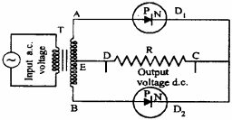
2. Working function:
When a.c. voltage is applied on primary coil of step – up transformer T, a.c. voltage induces in secondary coils. In first half cycle, A is at positive and B is at negative potential with respect to E. Therefore, diode D1 becomes forward – biased and current flows in load resistance R from C to D. This time point B is at lower potential relative to E, therefore D2 is at reverse biased.
In second half cycle, A is at negative and B is at positive potential relative to E. D1 gets reverse – biased and stops working where D2 is at forward – biased and allows current to flow from C to D. In this way in both the half cycles, current flows through the load resistance and diode behaves as full-wave rectifier.
Question 10.
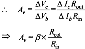
Draw a labelled circuit to explain the use of P – N – P transistor in CE mode as an amplifier. Obtain expression for current gain, voltage gain and power gain.
Answer:
See Long Answer Type Question No. 4 for circuit diagram and working.
1. Current gain : The ratio of change in collector current to change in base current is called current gain. It is denoted by β.
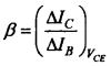
2. Voltage gain: The ratio of change in output voltage ∆VCE to change in input voltage ∆VBE is called voltage gain AV.
![]()
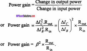
3. Power gain : The ratio of change in output power to change in input power is called power gain.
Question 11.
What is oscillator? Explain the function of transistor as an oscillator.
Or
What is an oscillator? Draw necessary circuit diagram to show the use of transistor as an oscillator.
Or
What is an oscillator? Explain use of transistor as oscillator under following points:
- Labelled circuit diagram
- Working.
Answer:
Oscillator : Oscillator is a device which can produce high frequency oscillations.
Use of transistor as an oscillator : A circuit is given in which a transistor is used in common emitter configuration.
Theory:
By proper coupling a tank circuit (L1 – C1 circuit) and feedback circuit a transistor oscillator can be made. A tank circuit is joined between the collector and key K. C1 is a variable capacitor with the help of which any desired frequency can be obtained in tank circuit. An inductor L1 is added between the base and emitter. Inductor L is coupled properly with inductor L1.
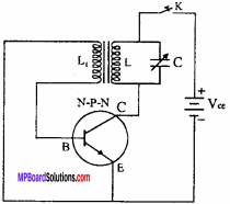
Working function:
When key K is pressed electric oscillation starts in tank circuit. As L is coupled with L1, e.m.f. is produced in inductor L due to induction of which value changes in magnitude and direction. In this way increase in base potential causes increase in collector current which helps oscillation in tank circuit. As a result, tank circuit L1 – C1 oscillates with constant amplitude. Energy wasted is recovered from the battery.
Frequency of oscillation, ν = \(\frac { 1 }{ 2\pi \sqrt { { L }_{ 1 }{ C }_{ 1 } } }\)
Where, L1 = Induction of inductor L,C1 = Capacity of capacitor C.
Semiconductor Electronics: Materials, Devices and Simple Circuits Numerical Questions
Question 1.
In a P – N junction, width of depletion layer is 10-6 m and potential barrier is 0.7 Volt. Calculate the barrier electric field.
Solution:
Given : d = 10-6 m, V = 0.7 volt
Formula: E = \(\frac {V}{d}\)
∴E = \(\frac { 0.7 }{ { 10 }^{ -6 } }\), or E = 7 x 10⁵ volt/metre.
Question 2.
In a P – N junction diode if the potential is changed by 0.12 volt then cunrent changes by 1.5 mA. Find out dynamic resistance of diode.
Solution:
Given : ∆V = 0.12 volt, ∆ I = 1.5 mA = 1.5 x 10⁻³A
Formula : rd = \(\frac {∆V}{∆d}\)
or rd = \(\frac { 0.12 }{ 1.5\times { 10 }^{ -3 } }\)
= \(\frac {0.12}{1.5}\) x 103 = 80 ohm.
![]()
Question 3.
The current gain of a transistor in CB mode is 0.987. What will be its current gain in CE mode?
Solution:
Given : α = 0.987
Formula : β = \(\frac {α}{1 – α}\)
β = \(\frac {0.987}{1 – 0.987}\) = 75.93.